

[ad_1]
Utilizing holograms, a nanoscale 3D printer can now quickly fabricate complicated gadgets with particulars smaller than a wavelength of seen mild, a brand new research finds. This analysis can quickly manufacture nanotechnological arrays of wires, lenses, rotating magnetic gears, and different buildings—suggesting purposes in electronics, photonics, microrobotics and extra.
Presently, essentially the most exact 3D-printing approach for manufacturing nanoscale objects with complicated shapes is probably going two-photon lithography. This strategy depends on liquid resins that solidify solely once they take up two photons of sunshine on the identical time as a substitute of only one. This permits exact fabrication of things with voxels—the 3D equal of pixels—solely a few dozen nanometers in measurement.
Nonetheless, two-photon lithography has confirmed too gradual and costly for large-scale sensible purposes. This has largely rendered it an costly laboratory device to provide microscopic prototypes.
The brand new methodology can manufacture complicated, microscopic 3D objects equivalent to letters, numbers, rings, lenses, and gears that may be remotely managed by making use of a magnetic discipline.
Earlier analysis has sought to separate the laser beam utilized in two-photon lithography into a number of focal factors to hurry up fabrication. Nonetheless, this technique usually nonetheless achieves printing speeds of solely about 10,000 voxels per second and fewer than 0.1 cubic millimeters per hour. Furthermore, this strategy is normally not capable of management every particular person laser’s focus, and so can’t produce extremely variable buildings.
Now a brand new two-photon lithography approach can print nanoscale 3D objects at speeds of as much as 2 million voxels per second and 4.5 to 54 cubic millimeters per hour. As well as, it achieved a decision of as much as 90 nanometers, the most effective seen but in high-throughput two-photon lithography, the scientists famous. Furthermore, the workforce’s new course of can concurrently function as much as 2,000 individually programmable laser foci to manufacture complicated buildings, essentially the most seen but in high-throughput two-photon lithography, they added.
“The rise in throughput means the fee is considerably lowered, and the expertise can now be used for industrial-scale purposes at a extra affordable worth and fabrication charge,” says research senior creator Shih-Chi Chen, an optical scientist and mechanical engineer on the Chinese language College of Hong Kong.
Solidifying the resin utilized in two-photon lithography requires extraordinarily excessive laser intensities. Utilizing a number of laser foci will increase the laser energy required, and the lasers usually utilized in two-photon lithography can barely present the facility wanted to help greater than 50 foci. In distinction, the brand new methodology used a near-infrared laser with a peak energy of roughly 10 gigawatts.
Often, two-photon lithography depends on foci that obtain about 10,000 low-power laser pulses with a view to totally solidify a voxel. Nonetheless, the brand new approach makes use of a laser that fires tens to a whole bunch of hundreds of occasions slower than the lasers usually utilized in two-photon lithography. To compensate, the brand new approach makes use of a single pulse to solidify every voxel. This required vital tinkering with the light-sensitive resin to optimize its printing high quality, the scientists mentioned.
“We achieved the most effective decision with single-pulse publicity, which is completely reverse to the traditional strategy to realize excessive decision—that’s, low common energy and lengthy publicity time,” Chen says.
The brand new methodology fires a thousand 100-femtosecond-long pulses per second, bouncing these pulses off a digital micromirror system that shows a hologram. The scientists may use the hologram to divide every laser pulse into as much as 2,000 foci with individually controllable power, location and section that would function concurrently in parallel.
In experiments, the researchers confirmed their new methodology may manufacture complicated, microscopic 3D objects equivalent to letters, numbers, rings, lenses, and eggbeater-like buildings. In addition they fabricated magnetic gears they might remotely management by making use of a magnetic discipline.
 These 14 photographs reveal the vary of nanostructures the brand new holographic approach can fabricate, together with magnetic nanoscale gear wheels that may very well be remotely moved by making use of a magnetic discipline [insets m and n].Chinese language College of Hong Kong
Within the new research, the scientists additionally revealed they might modify the laser energy of every focus to realize 11 totally different depth ranges. This “gray-scale management” could discover use in adjusting the solidity and mechanical properties of every voxel. The brand new approach displayed gray-scale management with an accuracy of greater than 99 %, the best seen but in parallel two-photon lithography, the scientists famous.
As well as, the researchers reported, the brand new methodology yields the best vitality effectivity but in two-photon lithography. Whereas different strategies demand an working energy of roughly 1.5 to 4 watts, the brand new methodology requires solely a median energy of 400 milliwatts to function 2,000 foci.
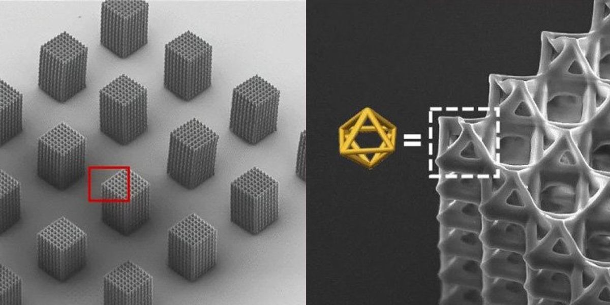
One potential utility for nanoscale 3D printing is fabricating metastructures—materials whose buildings possess repeating patterns at scales which might be smaller than the wavelengths of no matter drive they’re designed to affect. Optical metastructures, that are designed to govern electromagnetic radiation, can bend mild in surprising methods, leading to invisibility cloaks and different gadgets.
One of many biggest challenges with analysis into metastructures is manufacturing objects containing subfeatures lower than a micrometer in measurement however, on the entire, are many hundreds of occasions as giant as their subfeatures. In experiments, the scientists revealed their new approach may fabricate a grid roughly 1 cubic millimeter in measurement made up of greater than 680,000 cells with subfeatures as small as 700 nanometers.
The researchers are actually exploring utilizing AI to generate optimum fabrication procedures with their new approach. The purpose is for the merchandise to “have higher structural integrity, power, and uniformity,” Chen says.
The scientists detailed their findings on-line 27 March within the journal Nature Communications.
From Your Website Articles
Associated Articles Across the Internet
[ad_2]
Source link
